The use of thermal cameras optimises inspection of semiconductor
March 23, 2010
Today, semiconductor manufacturers looking for the best performance, almost always with great restrictions of time. Any type of defect You should find in the design phase and during the process of prototyping to manufacturing. Control of defects, based on the cameras thermal SWIR, provides accurate information on the stability of the process and the success of the final quality of the product, thanks to the ability to detect low levels of photon emission found in defects in semiconductor networks. The defects in the semiconductor crystal structures are exposed by the low emission in near infrared (SWIR) spectrum. This makes the latest cameras and high-sensitivity SWIR in the most suitable for a quick and accurate location of defects. This uses the procedure known as photoemission microscopy (PEM). It's a new technique of analysis of defects that detects light of different wavelengths emitted by defective parts, normally not visible to the eye, as low level. The photoemission microscopy uses an intensification of image technology to amplify the light emitted by the defective parts. The image of the resulting radiation overlaps with their corresponding image of the surface (of a chip for example), so that the place of issue coincides with the exact location of the defect. An infrared camera and a computer are used to carry out this function. At this time, other failure analysis techniques are used to find the responsible for physical anomaly by the abnormal light emission. This configuration can be extended to a spectroscope, replacing the beam splitter and the filter with a suitable dispersion element (basically a filter).
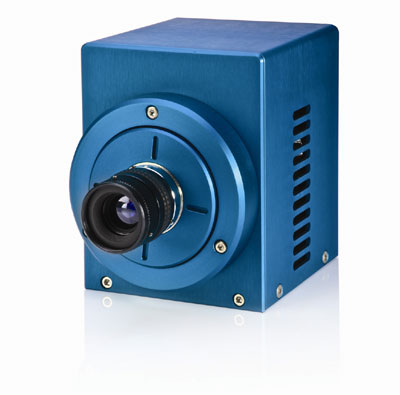
Photoemission microscopy applications include detection of electroluminescence previously unknown or not detectable; detection of abundant luminescence in unions with breakdowns, defects lace, flows caused by transistor MO and the detection of the flow of current through SiO2 dielectric electroluminescence and without. From Infaimon, he has collaborated with several engineering in the development of quality control in semiconductor projects using Xenics Xeva 1.7-320 camera. The first is a thermal camera to capture images in the spectrum of wavelengths between 0.9 and 2.5 micrometers, and combining a detector Ingaes Thermo-Electrically cooled and the electronics of control and communication, in a very confined space.
